MIPS mini-Processor
Download [starter]
Introduction
In this project, you will implement a basic version of a MIPS processor. The assignment is organized into two parts: A and B.
In part A (tasks 1 to 3), you are required to build an “Arithmetic Logic Unit (ALU)” and a “Register File” for a basic MIPS processor, as well as an implementation of a single-cycle datapath for executing addi instructions. In Part B (Task 4), you need to add other circuit components to your basic processor to produce an advanced version that will execute “real” MIPS instructions!
Start by downloading the startup file and unzipping its contents to the directory of your choice. Here is the list of files you must have:
proj_starter
  ├── cpu
  │   ├── alu.circ
  │   ├── branch_comp.circ
  │   ├── control_logic.circ
  │   ├── cpu_pipelined.circ
  │   ├── cpu_single.circ
  │   ├── imm_gen.circ
  │   ├── mem.circ
  │   └── regfile.circ
  ├── harnesses
  │   ├── alu_harness.circ
  │   ├── regfile_harness.circ
  │   ├── run_pipelined.circ
  │   ├── run_single.circ
  │   ├── test_pipelined_harness.circ
  │   └── test_single_harness.circ
  ├── logisim-evolution.jar
  ├── tests
  │   ├── part_a
  │   │   ├── ...
  ╎   ╎   ╎
  │   │   └── ...
  │   └── part_b
  │       ├── ...
  ╎       ╎
  │       └── ...
  └── test_runner.py
Part A: Initial CPU draft
Task 1: Arithmetic and Logic Unit (ALU)
Your first task is to create an “Arithmetic and Logic Unit (ALU)” that supports all the operations required by our ISA instructions (see next section).
The provided skeleton file alu.circ shows that your ALU should have three inputs:
| Input name | Width in bits | Description |
|---|---|---|
| A | 32 | Data on input A for ALU operation |
| B | 32 | Data on input B for ALU operation |
| ALUSel | 4 | Selects which operation the ALU should perform (see below for list of operations with corresponding switch values). |
… and two outputs
| Output name | Width in bits | Description |
|---|---|---|
| Zero | 1 | This output is set when the difference between inputs A and B is zero |
| Result | 32 | ALU operation result |
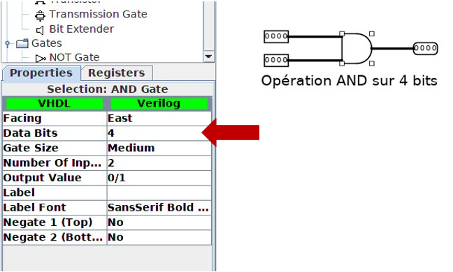
NOTES: In the « RAM and CPU » lecture slides, it is shown that and in order to build a multi-bit ALU (8 bits is given as an example), one needs to duplicate a 1-bit circuit and “link” these copies together to get an n-bit ALU. Good news! you don’t have to do that in this assignment… Logisim already does that for you! Simply choose the right bit width for your components’ inputs/outputs and your are done (see figure below).
The list below shows the operations (and the associated ALUSel values) that your ALU must be able to perform. You can use any Logisim block or integrated function to implement your circuits (There is no need to reimplement the adder, shifter or multiplier circuits! Use the circuit blocks provided by Logisim for this purpose).
| ALUSel | Instruction | Description | Note |
|---|---|---|---|
| 0 | add | Result = A + B |
|
| 1 | and | Result = A & B |
|
| 2 | or | Result = A | B |
|
| 3 | xor | Result = A ^ B |
|
| 4 | srl | Result = A >> B |
Unsigned right shift |
| 5 | sra | Result = A >> B |
Signed right shift |
| 6 | sll | Result = A << B |
|
| 7 | — | — | Not used |
| 8 | slt | Result = A < B ? 1 : 0 |
Signed comparison |
| 9 | sltu | Result = A < B ? 1 : 0 |
Unsigned comparison |
| 10 | mul | Result = (A * B)[31:0] |
Signed mult (31..0) |
| 11 | mulhu | Result = (A * B)[63:32] |
Unsigned mult |
| 12 | sub | Result = A - B |
|
| 13 | — | — | Not used |
| 14 | mulh | Result = (A * B)[63:32] |
Signed mult (63..32) |
Hints :
-
The MIPS
addoperation is already implemented for you; feel free to use a similar structure to build the other functions. -
When implementing
mulandmulh, note that the multiplication circuit block in Logisim has a “Carry Out” output that might be useful (the adder block also has this output, but you won’t needed it for this project). -
“Splitters” and “Bit extenders” could be very useful when implementing shift operations.
-
Use tunnels extensively for the wirings! This will help you avoid crossing wires inadvertently (and causing unexpected errors).
-
A multiplexer (MUX) can be useful in deciding which output of which component you want to transmit. I.e. process the inputs in all components simultaneously, then, depending on the chosen operation, select the correct output to transmit.
CAUTION
You can make any changes you see fit to alu.circ, but the circuit's inputs and outputs must obey the behavior specified above. Additionally, your alu.circ must fit into the provided harness circuit alu_harness.circ. This means you should AVOID moving the inputs or outputs of the alu.circ circuit. If you need more space, use tunnels!
If you create additional subcircuits, they must also be in alu.circ (i.e. you should not create new ".circ" files).
To check that your modifications to alu.circ have not broken the input/output correspondences between your circuit and the harness, open the alu_harness.circ file in Logisim and make sure that there are no errors (i.e. no red or orange wires).
Testing your ALU
A set of consistency tests for your ALU is provided in the tests/part_a/alu folder. Running the test_runner.py script (see below) will run the ALU tests and output the results to the tests/part_a/alu/student_output folder.
$ python3 test_runner.py part_a alu
Also provided is a binary_to_hex_alu.py script that helps to convert the outputs of the ALU into a readable format. To use the script, type the following in the console:
$ cd tests/part_a/alu
$ python3 binary_to_hex_alu.py PATH_TO_OUTPUT_FILE
For example, to view the content of the reference output file reference_output/alu-add-ref.out, do the following:
$ cd tests/part_a/alu
$ python3 binary_to_hex_alu.py reference_output/alu-add-ref.out
To see the difference between your circuit output and the reference solution, put the readable outputs into new .out files and compare them with the diff command (cf. man diff in a console). For example, for the alu-add test, you can do:
$ cd tests/part_a/alu
$ python3 binary_to_hex_alu.py reference_output/alu-add-ref.out > reference.out
$ python3 binary_to_hex_alu.py student_output/alu-add-student.out > student.out
$ diff reference.out student.out
Task 2: Registers File
In this task, you will implement the $0 – $31 registers specified in the MIPS architecture. To ease the implementation, eight registers will be ‘exposed’ for testing and debugging purposes (see the list below). Please ensure that the values of these registers are attached to the appropriate outputs in regfile.circ.
Your “Registers File” should be able to read from or write to the registers specified in a MIPS instruction without affecting other registers. There is one notable exception: your “Registers File” should NOT write to the $0 register even if an instruction attempts to do so. As a reminder, register $zero should ALWAYS be set to 0.
The ‘exposed’ registers and their corresponding numbers are indicated below.
| Register's number | Register's name |
|---|---|
| 4 | $a0 |
| 8 | $t0 |
| 9 | $t1 |
| 10 | $t2 |
| 16 | $s0 |
| 17 | $s1 |
| 29 | $sp |
| 31 | $ra |
A skeleton circuit of the “Registers File” is provided in regfile.circ. The circuit has six inputs:
| Input's name | Width (in bits) | Description |
|---|---|---|
| Clock | 1 | Input providing the clock. This signal can be routed to other subcircuits or directly connected to the clock inputs of the memory units in Logisim, but must not be connected to logic gates in any way (i.e. do not invert it, do not AND it, etc.) |
| RegWEn | 1 | Enables data writing on the next rising edge of the clock |
| rs | 5 | Selects which register value is sent to output Read_Data_1 (see below) |
| rt | 5 | Selects which register value is sent to output Read_Data_2 (see below) |
| rd | 5 | Selects which register will be updated with the content from Write_Data on the next rising edge of the clock (provided that RegWEn is 1) |
| Write_Data | 32 | Data to be written to the register selected by rd on the next rising edge of the clock (provided that RegWEn is 1) |
The “Registers File” in regfile.circ also has the following outputs:
| Output's name | Width (in bits) | Description |
|---|---|---|
| Read_Data_1 | 32 | Returns the content of register rs |
| Read_Data_2 | 32 | Returns the content of register rt |
| Value ra | 32 | Returns the content of register ra (output used for debugging and testing) |
| Value sp | 32 | Returns the content of register $sp (output used for debugging and testing) |
| Value t0 | 32 | Returns the content of register $t0 (output used for debugging and testing) |
| Value t1 | 32 | Returns the content of register $t1 (output used for debugging and testing) |
| Value t2 | 32 | Returns the content of register $t2 (output used for debugging and testing) |
| Value s0 | 32 | Returns the content of register $s0 (output used for debugging and testing) |
| Value s1 | 32 | Returns the content of register $s1 (output used for debugging and testing) |
| Value a0 | 32 | Returns the content of register $a0 (output used for debugging and testing) |
The test outputs at the top of the circuit in regfile.circ are there for testing and debugging purposes. A real “Registers file” does not have these outputs! Make sure they are properly connected to the indicated registers because if they are not, the autograder will not be able to evaluate your assignment correctly.
Hints :
-
To avoid repetitive (and boring) work, start by creating a fully functional register and then use it as a template to build the others.
-
It is recommended not to use the “
enable” input on your MUXes. In fact, you can even disable this feature from the Logisim panel. It is also recommended to set the “three-state?” property to “off”. -
See step 4 of “Design example 2” in the “Logisim tutorial” document to see what each input/output of a Logisim register corresponds to.
-
As with the ALU task, multiplexers will be very useful (demultiplexers, too).
-
What happens in the “Registers File” after a machine instruction is executed. Which values change? Which values stay the same? Registers are triggered by a clock - what does this mean?
-
As a reminder, registers have an “
enable” input as well as a “clock” input. -
What is the value of register
$0?
CAUTION
You can make any changes you want to regfile.circ, but the inputs and outputs of the circuit must follow the specifications given above. In addition, your regfile.circ must fit into the provided harness circuit regfile_harness.circ. This means that you must be careful NOT to move the inputs or outputs of the regfile.circ circuit. If you need more space, use tunnels!
If you create additional subcircuits, they must also be in regfile.circ (i.e. do not create new .circ files).
To verify that your changes have not broken the input/output mappings between your circuit and the harness, open the regfile_harness.circ file and make sure there are no wiring errors.
Testing your “Registers File“
A set of validity tests are provided in the tests/part_a/regfile folder. Running the tester (see below) will also run the ALU tests and output the results to the tests/part_a/regfile/student_output folder.
$ python3 test_runner.py part_a regfile
Also provided is a binary_to_hex_regfile.py script which works in a similar way to the binary_to_hex_alu.py script introduced in task #1.
Task 3: The addi instruction
In this third and final task for Part A, you need to implement a Datapath that can execute addi instructions! You can implement other additional instructions if you wish, but you will only be graded if the addi instructions execute correctly for this part of the project.
Description of the subtasks
The Memory Unit (mem.circ)
The Memory Unit (found in mem.circ) is already implemented for you! However, the addi instruction does NOT use the Memory Unit, so you can ignore this component for part A.
The Branching Unit (branch_comp.circ)
The branch_comp.circ file provides a skeleton circuit for the “Branching Unit”, but since the addi instruction does NOT use this unit, you can ignore it for part A.
The Immediate Unit (imm_gen.circ)
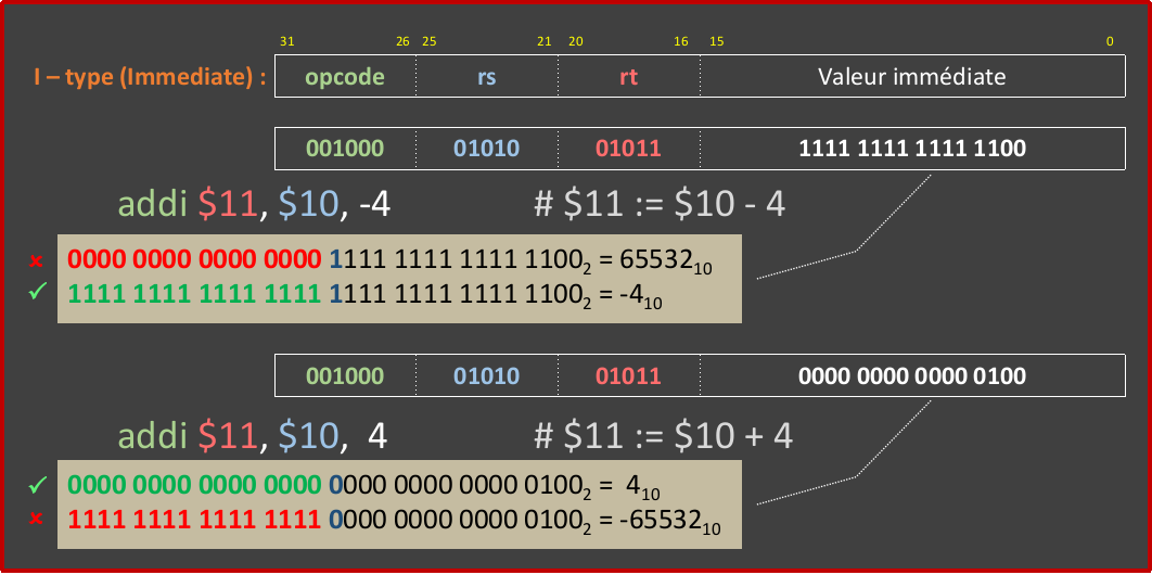
The imm_gen.circ file provides a skeleton circuit for the “Immediate Unit”. The addi instruction uses this unit. However, since this is the only instruction to be designed in this part of the project, you can simply lay out the wires necessary to generate the immediate associated with an addi instruction without worrying about other types of immediates. See the image below to see how the immediate of the addi instruction should be generated:
WARNING
To implement the "Immediate Unit", edit the imm_gen.circ file and not the imm_gen virtual circuit included in cpu_*.circ. Note that each time you edit the imm_gen.circ circuit, you must close and open the cpu_*.circ file to apply the changes to your CPU.
Here is a summary of the unit’s inputs and outputs:
| Name | Direction | Width (in bits) | Description |
|---|---|---|---|
| inst | Input | 32 | The instruction currently being executed |
| ImmSel | Input | 2 | A Selector to choose between different immediate generators |
| Imm | Output | 32 | Generated Immediate |
The Control Unit (control_logic.circ)
The control_logic.circ file provides a skeleton circuit for the “Control Unit”. Designing your Control Unit will probably be your biggest challenge in Part B of this assignment. For Part A, since addi is the only instruction you will implement, you can simply assign a constant for each control signal. However, as you progress through your implementation of addi, think about where you should make future modifications/additions to support other instructions besides addi.
WARNING
To implement the "Control Unit", edit the control_logic.circ file and not the control_logic virtual circuit included in cpu_*.circ. Note that each time you edit the control_logic.circ circuit, you must close and open the cpu_*.circ file to apply the changes to your CPU.
CAUTION
During the implementation of your "Control Unit", you can add extra input or output ports to control_logic.circ. You can also use the already provided ports (or a subset of them) depending on the needs of your implementation. That said, do not modify or delete any of the existing ports during this process.
The Processor (cpu*.circ)
The starter kit also provides skeletons for your processor in cpu*.circ. For Part A of the project, your processor must be able to execute the addi instruction using a two-stage pipeline, with “Instruction Fetch (IF)” in the first stage and ( ID – EX – MEM – WB ) in the second stage. First, using your own implementations of the ALU and “Registers File” from task 1 & 2, implement a single-cycle datapath (use the skeleton file cpu_single.circ for this mode of execution). Once your non-pipelined processor is working properly, you can make a copy of it into cpu_pipelined.circ and then modify your processor to produce a pipelined version.
Your processor will be inserted into the test_single_harness.circ harness (or test_pipelined_harness.circ, as appropriate) that contains the memory unit. This harness is in turn inserted into the run_single.circ (resp. run_pipelined.circ) test socket which provides the instructions (i.e. machine code) to the processor.
As an output, your processor will emit the address of an instruction to be read (i.e. fetched) from the instruction memory (IMEM). The fetched instruction is then transmitted to the processor in the appropriate input.
Also as an output, the processor will emit the address of a data to read from DMEM memory and a WRITE_ENABLE signal set to 1 if a store is requested instead. If data is read from DMEM, it is transmitted to the processor in the appropriate input (i.e. READ_DATA).
Essentially, the test_*_harness.circ and run_*.circ harnesses simulate a data (DMEM) and instruction (IMEM) memories respectively. Take the time to familiarise yourself with how they work to get an overall idea of the simulator.
CAUTION
The test_*_harness.circ harnesses will be used by the consistency tests provided in the starter kit, so make sure that your cpu_*.circ processor fits properly into these sockets before testing your circuits, and especially when submitting your work for grading
As with the ALU and the "Registers File" tasks, make sure NOT to move the input or output ports!
The processor has three inputs that come from the harness:
| Input's name | Width (in bits) | Description |
|---|---|---|
| READ_DATA | 32 | Data retrieved from DMEM memory at the address given in DMEM_ADDRESS (see below). |
| INSTRUCTION | 32 | The instruction fetched from IMEM memory at the address indicated by IMEM_ADDRESS (see below). |
| CLOCK | 1 | Input providing the clock. As already mentioned in the “Registers File” task, this signal can be routed to other subcircuits or directly connected to the clock inputs of the memory units in Logisim, but must not be connected to logic gates in any way (i.e. do not invert it, do not apply the “AND” gate on it, etc.). |
…and provides the following outputs for the harness:
| Output's name | Width (in bits) | Description |
|---|---|---|
| ra | 32 | Returns the content of register ra (output used for debugging and testing) |
| sp | 32 | Returns the content of register $sp (output used for debugging and testing) |
| t0 | 32 | Returns the content of register $t0 (output used for debugging and testing) |
| t1 | 32 | Returns the content of register $t1 (output used for debugging and testing) |
| t2 | 32 | Returns the content of register $t2 (output used for debugging and testing) |
| s0 | 32 | Returns the content of register $s0 (output used for debugging and testing) |
| s1 | 32 | Returns the content of register $s1 (output used for debugging and testing) |
| a0 | 32 | Returns the content of register $a0 (output used for debugging and testing) |
| DMEM_ADDRESS | 32 | Data Memory (DMEM) address |
| WRITE_DATA | 32 | Data to store into DMEM |
| WRITE_ENABLE | 4 | Enables or disables writting into DMEM |
| IMEM_ADDRESS | 32 |
This output holds the address of the instruction to retrieve from IMEM (in run_*_harness.circ). The fetched instruction is fed to the INSTRUCTION input port of the CPU |
Implementation Guidelines for the single-cycle processor
These guidelines will help you implement the addi instruction in your cpu_single.circ processor. Each section below contains questions to think about and important hints. It is necessary to read and understand each question before moving on to the next one! You can even check the answers by clicking ▶ if you are unable to find the answers yourself.
Recall the five steps of executing an instruction in a MIPS processor:
- Instruction Fetch (IF)
- Instruction Decode (ID)
- Instruction Execution (EX)
- Read from (resp. Write to) Data Memory (MEM)
- Eventually Write Back to the “Registers File” (WB)
Step 1: Instruction Fetch (IF)
The main question that arises at this stage is “How to get the current instruction?”. We have seen in lecture Datapath that instructions are stored in the Instructions Memory (IMEM), and each of these instructions is accessible via an address.
A simple implementation of the PC register is provided in cpu_*.circ. This implementation does not take into account the jump and branch instructions that you will need to implement in Part B of this project. But for now, only addi instructions need to be handled by the processor.
Recall however that you will eventually implement a 2-stage pipelined processor, so that the IF stage is separated from the remaining stages. What circuit separates the different stages in a pipeline? More precisely, what circuit separates IF from the next stage? Is there anything you need to add here?
Step 2: Instruction Decoder (ID)
Once the “IF” stage is implemented, the fetched instruction should be available at the INSTRUCTION input port of the processor. The second step is therefore to decompose this instruction in order to determine what to do with it in the subsequent execution steps.
Step 3: Executing the instruction (EX)
The execution stage is where the computation is done.
Step 4: Read from/write to Data Memory (MEM)
The MEM step is where the Data Memory (DMEM) can be modified using data store instructions or read using data load instructions. Since the addi instruction does not need accesss to DMEM, we can ignore this part of the circuit for now and continue with the next step of execution.
Step 5: Writing back to the “Registers File” (WB)
The WriteBack step is required when the results of an operation are to be saved to a register in the “Registers File”.
If you did all the steps correctly, you should have a single-cycle processor (cpu_single.circ) that works for addi instructions 🎉. Run python3 test_runner.py part_a addi_single from the terminal and check if your implementation works correctly!
Guidelines for a two-stage pipelined processor
Now it’s time to turn your single-cycle processor into a “pipelined” version! For this project, you need to implement a two-stage pipeline, which is still conceptually similar to the five-stage pipeline introduced in the “Pipelining” lecture. The two stages to implement are:
- Instruction Fetch (PIF): An instruction is fetched from Instructions Memory (IMEM).
- Instruction Execution (PEX): The instruction is decoded, executed, and validated (i.e. result saved). This is a combination of the last four stages (ID, EX, MEM, and WB) in a single-cycle processor.
Since the instruction decoding and execution steps are handled in the PEX stage, your pipelined addi processor will be more or less identical to its « single-cycle » version, except for the one clock cycle startup latency. We will, however, apply the pipeline design rules seen in class in order to prepare our processor for Part B of this project.
Some points to consider for a two-stage pipeline design:
-
Will the PIF and PEX stages have the same or different
PCvalues? -
Do you need to store the
PCbetween pipeline stages?
On the other hand, we will get a bootstrapping problem here: during the first execution cycle, the registers introduced between the different pipeline stages are initially (empty), but the void does not exist in hardware. How will we handle this first dummy instruction? What would the void correspond to in our processor? I.e. to what value should we initialise the newly introduced registers in order to “do nothing” during the first execution cycle?
Sometimes Logisim automatically resets the registers to zero at startup (or on reset); which, for our bootstrapping problem, will simulate a nop instruction! Thanks Logisim! Don’t forget to go to « Simulate | Reset Simulation » to reset your processor.
After you have « pipelined » your processor, you should be able to pass the python3 test_runner.py part_a addi_pipelined tests. Note that the previous python3 test_runner.py part_a addi_single test should fail now (why? Check the benchmark outputs for each test and think about the effects of the pipeline registers on the different execution stages).
Understanding the tests
The cpu tests included in the startup circuits are copies of the run_*.circ files and contain instructions that have been previously loaded into the Instructions Memory (IMEM). When Logisim is run from the command line, your circuit is automatically started. Execution is clocked, your processor’s PC is updated, the fetched instruction is processed, and the values of each of the test circuit’s outputs are printed to the console.
Consider the addi-pipelined test folder as an example. Instruction Memory in the cpu-addi.circ circuit contains three addi instructions (addi $t0, $0, 5, addi $t1, $t0, 7 and addi $s0, $t0, 9). Open the tests/part_a/addi_pipelined/cpu-addi.circ file in Logisim and take a closer look at the different parts of the test circuit. At the top, you will see where the test_harness is connected to for the debug outputs. Initially, these outputs are all UUUUU, but this should not be the case once your cpu_pipelined.circ circuit is implemented.
The test_harness socket takes as input the clock signal clk and the Instruction provided by the Instruction Memory module. As output, the socket transmits (for display) the values of the debug registers from your processor circuit cpu_pipelined.circ. The additional output fetch_addr holds the address of the next instruction to fetch from Instruction Memory.
CAUTION
Do not move any of your processor's I/O and do not add additional I/O. This will change the shape of the processor's subcircuit in and therefore the connections with the test_harness module may not work properly anymore.
Under the test_harness module, you will see the Instruction Memory containing the hex machine code of the three addi instructions under test (0x20080005, 0x21090007, 0x21100009). The Instruction Memory takes an address (i.e. fetch_addr) and outputs the instruction stored at that address. In MIPS, fetch_addr is a 32-bit value, but since Logisim limits the size of ROM units to \(2^{24}\), we use a splitter to retrieve 24 bits of fetch_addr (i.e. the bit range 2..25, ignoring the lowest two bits).
So, when the test circuit is powered on, each tick of the clock drives the execution of the test_harness module and increments the counter called Time_Step (this counter is located to the right of the Instruction Memory, zoom out in Logisim if it is not visible on your screen).
At each tick of the clock, a command line execution of Logisim will print the values of each of your debug outputs to the terminal. The clock will continue to run until Time_Step equals the stopping constant for this test circuit (for this particular test file, the stopping constant is 4).
Finally, we compare the output of your circuit to the reference (i.e. expected) output; if your circuit output is different, the test will fail.
The addi tests
The “test runner” provided in the starter kit can be used to run two set of tests for the addi instruction: a set of tests for the single-cycle processor and a set of tests for the pipelined processor. You can run the test script for the “pipelined” version with the following command (replace pipelined with single to test the “single-cycle” version):
$ python3 test_runner.py part_a addi_pipelined # For a pipelined CPU
You can see the .s (MIPS) and .hex (machine code) files used for the test in tests/part_a/addi_pipelined/inputs.
To make it easier to interpret your output, a Python script (binary_to_hex_cpu.py) is also included. This script works like the binary_to_hex_alu.py and binary_to_hex_regfile.py scripts used in the ALU and in the “Registers File” design tasks (i.e. Tasks #1 and #2). To use the script, run:
$ cd tests/part_a/addi_pipelined
$ python3 binary_to_hex_cpu.py student_output/CPU-addi-pipelined-student.out
or, to view the reference output (i.e. what your circuit should print), run:
$ cd tests/part_a/addi_pipelined
$ python3 binary_to_hex_cpu.py reference_output/CPU-addi-pipelined-ref.out
Submit Part A of the assignment
Make sure again that you have not moved/modified your I/O ports and that your circuits fit into the provided test harnesses without any problems.
For the evaluation of this part of the project, you must submit a zipped file containing all the circuits that you need to implement (i.e. the alu.circ, regfile.circ, imm_gen.circ, control_logic.circ and cpu_*.circ circuits).
your_zipped_file.zip
 ├── alu.circ
 ├── regfile.circ
 ├── imm_gen.circ
 ├── control_logic.circ
 ├── cpu_single.circ
 └── cpu_pipelined.circ
If you’re using the VM provided for this course to do this project, you can zip two files (or more) file1.circ and file2.circ into a file named your_zipped_file.zip with the following steps:
- Open a terminal then, with the
cdbash command, go to the folder containing the files file1.circ and file2.circ. - Type the command:
zip your_zipped_file.zip file1.circ file2.circ
Then submit the file your_file.zip for evaluation. For this part of the project, the Autograder uses the same test files already provided in the starter kit. I.e. there are no hidden tests !
Part B: Processor design (advanced version)
Task 4: More instructions
In Task #3, you implemented a basic two-stage pipeline processor capable of executing addi instructions. Now, you will beef up your processor by implementing more instructions!
The Instruction Set Architecture (ISA) of the CPU
Below is a set of instructions your CPU must support and will be evaluated on. You are free to implement additional instructions if you wish but make sure, however, that none of your additional instructions affect the operation of the instructions specified here. Implementing additional instructions will not affect your score for this project.
| Instruction | Description | Operation | Type | Opcode/Func |
|---|---|---|---|---|
| add rd, rs, rt | Addition | R[rd] ← R[rs] + R[rt] | R | 0x0 / 0x20 |
| sub rd, rs, rt | Substraction | R[rd] ← R[rs] - R[rt] | R | 0x0 / 0x22 |
| addi rt, rs, imm | Addition (2nd param. : immediate) |
R[rt] ← R[rs] + imm± | I | 0x8 |
| mul rd, rs, rt | Multiplication | R[rd] ← (R[rs] x R[rt])[31:0] | R | 0x0 / 0x18 |
| mulh rd, rs, rt | Multiplication | R[rd] ← (R[rs] x R[rt])[63:32] | R | 0x0 / 0x10 |
| mulhu rd, rs, rt | Multiplication; (unsigned params) |
R[rd] ← (R[rs] x R[rt])[63:32] | R | 0x0 / 0x19 |
| and rd, rs, rt | logical AND | R[rd] ← R[rs] & R[rt] | R | 0x0 / 0x24 |
| or rd, rs, rt | logical OR | R[rd] ← R[rs] | R[rt] | R | 0x0 / 0x25 |
| xor rd, rs, rt | Exclusive OR | R[rd] ← R[rs] ^ R[rt] | R | 0x0 / 0x26 |
| andi rt, rs, imm | logical AND (2nd param. : immediate) |
R[rd] ← R[rs] & imm0 | I | 0xC |
| ori rt, rs, imm | logical OR (2nd param. : immediate) |
R[rd] ← R[rs] | imm0 | I | 0xD |
| xori rt, rs, imm | Exclusive OR (2nd param. : immediate) |
R[rd] ← R[rs] ^ imm0 | I | 0xE |
| sll rd, rt, sh | Logical left shift | R[rd] ← R[rt] << sh | R | 0x0 / 0x0 |
| srl rd, rt, sh | Logical right shift | R[rd] ← R[rt] >>> sh | R | 0x0 / 0x2 |
| sra rd, rt, sh | Arithmetic shift | R[rd] ← R[rt] >> sh | R | 0x0 / 0x3 |
| sllv rd, rt, rs | Logical left shift with register |
R[rd] ← R[rt] << rs | R | 0x0 / 0x4 |
| srlv rd, rt, rs | Logical right shift with register |
R[rd] ← R[rt] >>> rs | R | 0x0 / 0x6 |
| srav rd, rt, rs | Arithmetic shift with register |
R[rd] ← R[rt] >> rs | R | 0x0 / 0x7 |
| slt rd, rs, rt | Set if less than | R[rd] ← R[rs] < R[rt] ? 1 : 0 | R | 0x0 / 0x2A |
| sltu rd, rs, rt | Set if less than (unsigned) | R[rd] ← R[rs] < R[rt] ? 1 : 0 | R | 0x0 / 0x2B |
| slti rt, rs, imm | Set if less than (2nd param. : immediate) |
R[rt] ← R[rs] < imm± ? 1 : 0 | I | 0xA |
| sltiu rt, rs, imm | Set if less than (unsigned) (2nd param. : immediate) |
R[rt] ← R[rs] < imm± ? 1 : 0 | I | 0xB |
| j imm | Jump to Label | PC ← PC & 0xF0000000 | (imm << 2) | J | 0x2 |
| jal imm | Jump and link | $ra ← PC + 4; PC ← PC & 0xF0000000 | (imm << 2) |
J | 0x3 |
| jalr rd, rs | Jump to register and link | R[rd] ← PC + 4; PC ← R[rs] |
R | 0x0 / 0x9 |
| beq rt, rs, imm | Branch if equal | if (R[rs] == R[rt]) PC ← PC + 4 + (imm±<< 2) |
I | 0x4 |
| bne rt, rs, imm | Branch if not equal | if (R[rs] != R[rt]) PC ← PC + 4 + (imm±<< 2) |
I | 0x5 |
| lui rt, imm | Load upper immediate | R[rt] ← imm << 16 | I | 0xF |
| lb rt, imm(rs) | Load byte | R[rt] ← Mem( R[rs] + imm±, octet )± | I | 0x20 |
| lh rt, imm(rs) | Load half | R[rt] ← Mem( R[rs] + imm±, demi )± | I | 0x21 |
| lw rt, imm(rs) | Load word | R[rt] ← Mem( R[rs] + imm±, mot ) | I | 0x23 |
| sb rt, imm(rs) | Store byte | Mem( R[rs] + imm± ) ← R[rt][7:0] | I | 0x28 |
| sh rt, imm(rs) | Store half | Mem( R[rs] + imm± ) ← R[rt][15:0] | I | 0x29 |
| sw rt, imm(rs) | Store word | Mem( R[rs] + imm± ) ← R[rt] | I | 0x2b |
Notes :
- The writing imm± in the table above means “Apply a sign extension to the immediate imm”. The same remark applies to Mem(…)±. In this case the sign extension is applied to the byte or half-word retrieved from memory.
- The writing imm0 means “Extend with zeros the immediate imm”.
Data Memory DMEM (mem.circ)
The DMEM memory unit (provided in mem.circ) is already fully implemented and connected to your processor outputs in test_harness.circ! I.e. there is no need to add the memory unit (mem.circ) again to your implementation. Doing so will actually cause the testing scripts to fail, which will not be good for your score :(.
Note that the provided implementation of DMEM allows writing at the byte level to memory. This means that the Write_En signal is 4 bits wide and acts as a write mask. For example, if Write_En is 0b1000, then only the most significant byte of the addressed word in memory will be overwritten (e.g. sb $a0, 3($s0)).
On the other hand, the ReadData port will always return the word stored at the provided address. The memory unit ignores the two least significant bits in the address you provide and treats its input as a word address rather than a byte address. For example, if you enter the 32-bit address 0x00001007 (e.g. lb $a0, 7($s0), with $s0=0x0001000), it will be treated as word address 0x00001004, and you will get the 4 bytes at addresses 0x00001004, 0x00001005, 0x00001006 and 0x00001007 as output. So you need to implement the necessary mask logic to write only the required byte(s) into the “Registers File” (i.e. byte #3 for the example lb $a0, 7($s0)).
Finally, remember that unaligned RAM accesses will cause exceptions in MIPS. And since we do not implement any exception handling in this project, you can assume that only aligned address accesses are used for the lw, lh, sh and sw instructions. This means that the addresses used with the lw and sw (resp. lh and sh) instructions are multiples of 4 (resp. multiples of 2).
Voici un résumé des entrées et sorties de la mémoire :
| Name | Direction | Width (in bits) | Description |
|---|---|---|---|
| WriteAddr | Input | 32 | Address in memory (despite the name, it is used for read or write instructions) |
| WriteData | Input | 32 | Value to write to memory |
| Write_En | Input | 4 | The write mask for instructions that write to memory. Zero otherwise |
| CLK | Input | 1 | Input providing the CPU clock |
| ReadData | Output | 32 | Data read at the specified address |
The Branching Unit (branch_comp.circ)
The “Branching Unit” (skeleton provided in the branch_comp.circ file) should calculate the new value of the Program Counter (i.e. newPC) when the currently executing instruction is a branch or an jump to an “immediate”.
WARNING
To implement the "Branching Unit", edit the branch_comp.circ file and not the branch_com virtual circuit included in cpu_*.circ. Note that each time you modify the branch_comp.circ circuit, you will have to close and open cpu_*.circ to apply the changes to your CPU.
Here is a summary of the inputs and outputs of this unit:
| Name | Direction | Width (in bits) | Description |
|---|---|---|---|
| inst | Input | 32 | The current executing instruction |
| ximm | Input | 32 | The immediate returned by the Imm output of the “Immediate Unit” |
| PC | Input | 32 | The value of the PC register |
| zero | Input | 1 | The value returned by the zero output of the UAL |
| BrUn | Input | 2 | Selector to process the ‘right’ branch/jump instruction |
| newPC | Output | 32 | New value to transmit to the PC |
| BrJmp | Output | 1 | Indicates whether the instruction being processed is a branch/jump in the code |
The Immediate Unit (imm_gen.circ)
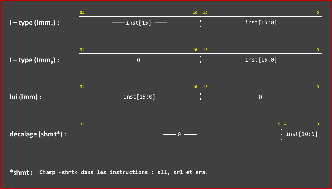
The imm_gen.circ file provides a skeleton circuit for the “Immediate Unit”. this unit should generate the “Immediate” constants associated with I-type instructions as well as the constant values encoded by the “shmt” field for shift instructions. See the figure below for how each immediate should be formatted in your processor:
WARNING
To implement the "Immediate Unit", edit the imm_gen.circ file and not the imm_gen virtual circuit included in cpu_*.circ. Note that each time you edit the imm_gen.circ circuit, you must close and open the cpu_*.circ file to apply the changes to your CPU.
Here is again a summary of the unit’s inputs and outputs:
| Name | Direction | Width (in bits) | Description |
|---|---|---|---|
| inst | Input | 32 | The instruction currently being executed |
| ImmSel | Input | 2 | A Selector to choose between different immediate generators |
| Imm | Output | 32 | Generated Immediate |
The Control Unit (control_logic.circ)
The control_logic.circ file provides a skeleton circuit for the “Control Unit”. In order to properly execute each MIPS instruction, control signals play a very important role in a processor (and this project!).
Review the lecture slides in Datapath and try traversing the data path with different types of instructions; when you encounter a MUX or other component, determine what selector or enable value you will need for that instruction.
CAUTION
During the implementation of your "Control Unit", you can add extra input or output ports to control_logic.circ. You can also use the already provided ports (or a subset of them) depending on the needs of your implementation. That said, do not modify or delete any of the existing ports during this process.
There are two main approaches to implementing the “Control Unit” so that it can extract the “opcode/func” of an instruction and set the control signals appropriately. The first method is hardwired control. This is generally the preferred approach for RISC architectures such as MIPS and RISC-V. Here, to implement truth and Karnaugh tables corresponding to the identified functions, we will use the logic gates “AND”, “OR” and “NOT” with the various components that can be built from these gates (such as MUXes and DEMUXes).
The other way is to use a ROM (read-only memory). Each instruction implemented by a processor is mapped to an address in this memory where the command and control word for that instruction is stored. An address decoder therefore takes an instruction as input (i.e. the “opcode/func”) and identifies the address of the word containing the control signals for that instruction. This approach is common in CISC architectures such as Intel/AMD x86-64 processors and offers some flexibility since it can be easily reprogrammed by changing the ROM’s content.
WARNING
To implement the "Control Unit", edit the control_logic.circ file and not the control_logic virtual circuit included in cpu_*.circ. Note that each time you edit the control_logic.circ circuit, you must close and open the cpu_*.circ file to apply the changes to your CPU.
The Processor (cpu*.circ)
The circuit in cpu_*.circ should implement the main data path and connect all the subcircuits together (ALU, Branching Unit, Control Unit, Immediate Unit, RAM and “Registers File”).
In Part A, you implemented a simple two-stage pipeline for your processor. You should realise that “data hazards” do NOT occur here because all data accesses happen in a single stage of the pipeline (i.e. the second stage).
However, since Part B of this project requires support for branch and jump instructions, there are some “control hazards” to deal with. In particular, the instruction immediately after a branch or jump statement is not necessarily executed if the branch is taken. This makes your task a bit more complex because by the time you realize that a branch or jump is being executed, you have already accessed the Instructions Memory and fetched the (possibly wrong) next instruction. So you must “roll back” the fetched instruction if the currently executing instruction will take the jump or branch.
You should only roll back the fetched instruction if a branch is taken (do not roll back otherwise). Instruction rollback MUST be accomplished by inserting a nop into the execution stage of the pipeline instead of the fetched instruction. Note that the instruction sll $0, $0, 0 or the associated machine code 0x00000000 is a nop instruction for our processor.
Some things to consider for your implementation:
- Will the PIF and PEX stages have the same or different PC values?
- Do you need to store the PC between different pipeline stages?
- Where to insert a possible
nopin the instruction stream? - What address should be requested next while the PEX stage is executing a
nop? Is this different than normal?
Testing your Processor
Some consistency tests are provided for your processor in tests/part_b/pipelined. To run the tests, type:
$ python3 test_runner.py part_b pipelined
You can view the .s (MIPS) and .hex (machine code) files used for testing in tests/part_b/pipelined/inputs.
You can also use the Python script binary_to_hex_cpu.py, as in task #3 of this project, to visualise and better interpret your results.
Submit part B of the assignment
If you finished task #4, you have completed part B of the project… Congratulations on your new processor 🎉!
Make sure again that you have not moved/modified your I/O ports and that your circuits fit into the provided test harnesses without any problems.
For the evaluation of this part of the project, submit a zipped file containing all the circuits that you need to implement
(i.e. the alu.circ, regfile.circ, branch_comp.circ, imm_gen.circ, control_logic.circ, cpu_single.circ and cpu_pipelined.circ.circuits).
your_zipped_file.zip
 ├── alu.circ
 ├── regfile.circ
 ├── imm_gen.circ
 ├── branch_comp.circ
 ├── control_logic.circ
 ├── cpu_single.circ
 └── cpu_pipelined.circ
If you’re using the VM provided for this course to do this project, you can zip two files (or more) file1.circ and file2.circ into a file named your_zipped_file.zip with the following steps:
- Open a terminal then, with the
cdbash command, go to the folder containing the files file1.circ and file2.circ. - Type the command:
zip your_zipped_file.zip file1.circ file2.circ
Then submit the file your_file.zip for evaluation. For this part of the project, the Autograder uses the same test files already provided in the starter kit and some additional hidden tests!