Logic circuit simulation software (Logisim)
Logisim is a tool for designing and simulating simple logic circuits. To launch the software on a lab machine (or the VM), run the following command from a terminal:
$ logisim
The basics
Let’s start by creating a very simple circuit of logic gates:
-
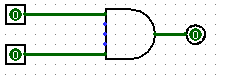
 Start by clicking on the “AND gate” button (left panel - “Gates” folder). You will notice that a shadow of an AND gate will follow your cursor movements. Click once in the main schematic window to place an AND gate.
 -
 Click on the “Pin” button (under “Wiring” - folder). Now, place two input pins to the left of your AND gate.
 -
Click on the “Pin” button again and place an output pin to the right of your AND gate. In the “Selection: Pin” panel (below left), change the Output? value to “Yes” and the “Facing” parameter to “West”. Your diagram should look like this:

-
 Click the “Select tool” button. Click and drag to connect the input pins to the left side of the AND gate. This will take several steps, as you can only draw vertical and horizontal wires. Simply draw a wire horizontally, release the mouse button, then click and drag down from the end of the wire to continue vertically. You can attach the wire to any pin on the left side of the AND gate. Repeat the same procedure to connect the output (right side) of the AND gate. After completing these steps, your circuit should look like this:
 You can also change the number of inputs of the “AND gate” by clicking on it with the “Select tool” and changing the “Number of Inputs” property in the “Properties” pane (below left).
 -
 Finally, click on the “Poke” tool then try clicking on the input pins of your circuit. Observe what happens. Does this match what you think an AND gate should do?
Subcircuits
Just as programs written in a high-level language can contain auxiliary functions, a circuit diagram can contain subcircuits. In this part, we will create several subcircuits to demonstrate their use.
-
Open the circuit ex1.circ (File | Open 🡒 ex1.circ). The NAND1 subcircuit window is automatically selected for you by Logisim.
-
In this window, create a simple
NANDcircuit with two input pins on the left side and one output pin on the right side. Do this without using the NAND gate found in the Gates folder (i.e. use only the AND, OR and NOT gates). You can change the labels of the inputs and outputs of the circuit by changing the “Label” property in the “Properties” pane. -
To create the additional subcircuits:
NOR,XOR,2-to-1 MUX, and4-to-1 MUX; double-click the circuit name in the “Design” pane on the left and repeat the steps you have done for theNANDsubcircuit. Do not use any built-in gates other than AND, OR, and NOT. However, once you have built a subcircuit, you can use it to create additional subcircuits (click once the created subcircuit in the “Design” pane and then click again in the Design window to insert it as a component).Note: For the
4-to-1 MUX,Sel0andSel1correspond to the 0th and 1st bits of the 2-bit selector, respectively.
Advanced features
Tunnels
A tunnel allows you to draw an “invisible wire” to connect two points together. Tunnels are grouped by labels (label names are case sensitive). They are used as follows:
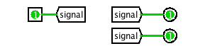
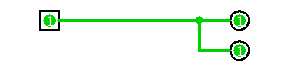
This has the same effect as:
It is highly recommend you use tunnels with Logisim, as they make your circuits much cleaner and therefore easier to understand/debug.
Splitter
This is an essential tool when designing circuits in Logisim. To demonstrate its use, you will build a circuit that manipulates an 8-bit number.
-
Create a new subcircuit and give it a name (e.g. “Ex2”).
-
Add an 8-bit input pin to your circuit and label it (e.g. “In1”).
-
Add a 1-bit output pin labeled “Out1” and an 8-bit output pin labeled “Out2” to your circuit.
-
Select the Splitter circuit from the “Wiring” folder in Logisim. This circuit takes an input bus and splits it into a set of smaller width buses. Conversely, it can also be used to recombine many sets of wires into a larger bus.
-
Before placing your circuit, change the “Bit Width In” property (bus width) to 8 and the “Fan Out” property (# of branches) to 3. If you move your cursor over the schematic, your cursor should look like this:

-
Now, select which bits to send to which branch of the splitter. The least significant bit is bit 0 and the most significant bit is bit 7. Make sure the bits 1 to 6 appear on branch #1 (the middle one) and leave the other two bits mapped to their default configuration. The “None” option means that the selected bit will not be mapped to any of the branches of the splitter.
-
Once the splitter is configured, you can place it in your circuit.
-
Route the
In1input pin to the splitter. Attach a 2-input AND gate to branches 0 and 2 of the splitter and route the output of this gate to the output pinOut1. -
Now, suppose the input is a number represented by “a sign bit and a magnitude”. Add the necessary logic so that
Out2represents the negative value of the inputIn1(Sign and magnitude is another way to represent signed values – like 2’s complement).
Bit Extender
When you change the width of a bus, you must use a bit extender. For example, consider the following implementation of extending an 8-bit bus to a 16-bit bus using splitter:

Whereas the following is much simpler, easier to read, and less error-prone:

Furthermore, consider the case of bit deletion. In the example below, an 8-bit bus is converted to a 4-bit bus by removing the 4 most significant bits:

Despite its name, a bit extender can also perform this same operation:

Design example 1: Build a 4-Bit “adder”
Now that you have gained some experience with Logisim, let’s design a slightly more complex circuit: a 4-bit adder!
An “adder” is a logic circuit used to perform additions. This circuit is very common in processors. It is used to perform arithmetic calculations in ALUs (i.e. Arithmetic Logic Units) but also to calculate the memory addresses for next instructions.
A full “adder” adds three numbers, often written as A, B and Cin; A and B are the operands, and Cin is the carry-in (possible result of a previous addition). The full “adder” is usually composed of a cascade of simple 8-bit, 16-bit, 32-bit, … adders.
In the notation below, A[4] indicates that the input is named “ A “ and is 4-bits wide. The input should not be named “ A[4] “ in Logisim!
| Add4 : | S = A + B + Cin; Cout = carry out |
|---|---|
| Operands : | A[4], B[4], Cin |
| Result : | S[4], Cout |
The S output is calculated by adding A , B and Cin. A , B and S are two’s complement numbers. If an overflow occurs, the Cout output should be set. In this case, the S output is the calculated value when all overflow errors are ignored.
Truth table of a 1-bit adder
A truth table shows how the output of a logic circuit should respond to various combinations of inputs. For example, if all the inputs to a full adder are “0s”, the outputs should also be “0s”. Complete the truth table below.
| A | B | Cin | Cout | S |
|---|---|---|---|---|
| 0 | 0 | 0 | 0 | 0 |
| 0 | 0 | 1 | ||
| 0 | 1 | 0 | ||
| 0 | 1 | 1 | ||
| 1 | 0 | 0 | ||
| 1 | 0 | 1 | ||
| 1 | 1 | 0 | ||
| 1 | 1 | 1 |
builing a “1-bit adder”
The above truth table can also be expressed using Boolean algebra.
   S =  A ⊕ B ⊕ Cin
Cout = (A ∧ B) ∨ (Cin ∧ (A ⊕ B) )
Hence the following diagram for our 1-bit adder.

A procedure called the Karnaugh table, named after Maurice Karnaugh, a telecommunications engineer at Bell Labs in 1953, makes it very easy to convert the truth table into a Boolean algebra representation. You can check out this article on Karnaugh tables to refresh your memory.
Implement this 1-bit adder in Logisim and verify that your circuit works correctly (use the truth table above for your comparisons).
Builing a “4-bit adder”
A 4-bit adder is made by cascading 4 1-bit adders, where the output of the current adder feeds the next adder.
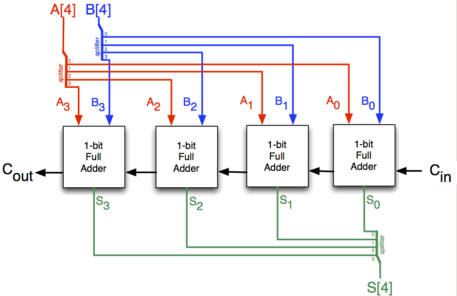
Build the 4-bit adder in Logisim by reusing the 1-bit adder you designed earlier as a subcircuit.
Hints:
- Use splitters
- Use tunnels
- Use probes to debug your circuit. You can connect probes to the input/output busses and set the values to display in decimal for quick verification. Refer to the help page for more information.
- Use subcircuits to create your 4-bit adder, and then optionally a 32-bit adder.
Design example 2: Implementing a finite state machine
Let’s now implement a circuit that continuously increments a value. The difference between this circuit and the circuits you’ve built so far is that it writes this value to a register (defining thus the state of the circuit).
-
Open the ex2.circ circuit (File | Open 🡒 ex2.circ) and navigate to the (initially empty)
AddMachinesubcircuit. -
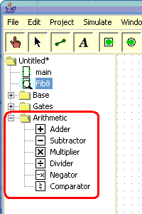
The Logisim “Arithmetic” library contains elements that perform basic mathematical operations:
-
Select the
Addersubcircuit from the “Arithmetic” library and place it in yourAddMachinesubcircuit. -
Select
Registerfrom theMemorylibrary and place a register in your subcircuit. Below is an image showing the components of a “logisim” register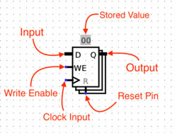
-
Connect a clock to your register. You can find the clock circuit element in the
Wiringfolder of the circuit browser. -
Connect the output of the adder to the input of the register and the output of the register to the input of the adder. You may get the error “Incompatible widths” when connecting the components. This means that the wire you are drawing is trying to connect two pins with different bit widths. Switch to the “Selection” mode if necessary (the “arrow” button pressed), then click on the adder component. The “Data Bits” property in the lower left field of the window shows/defines the number of bits of the input and output of the adder. Change this field if necessary to make the error disappear.
-
Connect a constant
1set to 8 bits to the second input of the adder. You can find theConstantcircuit element in theWiringlibrary. -
Add two output pins to your circuit so that you can monitor what is coming out of the adder and the register. The output of the adder should be connected to
ADD_OUTand the output of the register toREG_OUT. In the end, your circuit should look like this: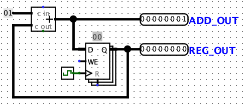
-
Now run your circuit from the Simulate | Ticks Enabled menu (or the keyboard combination Control + K). Your circuit should now display a binary counter.
-
If you want to run your circuit faster, you can change the “tick” frequency in Simulate | Tick Frequency.